.png)
.png)
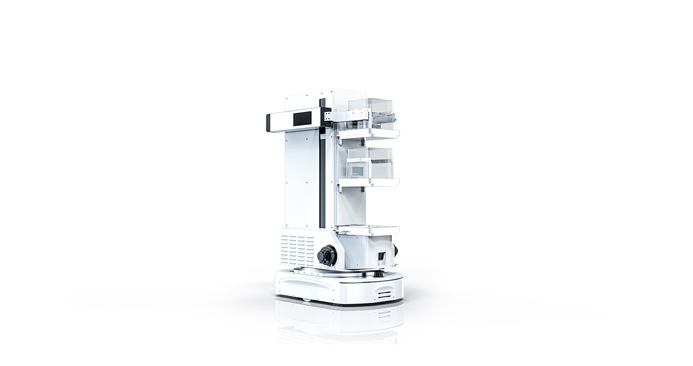
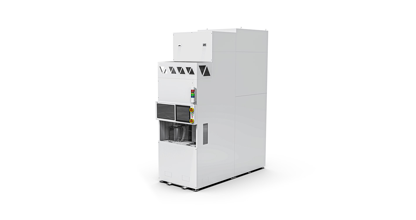
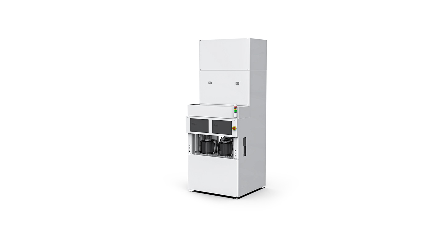
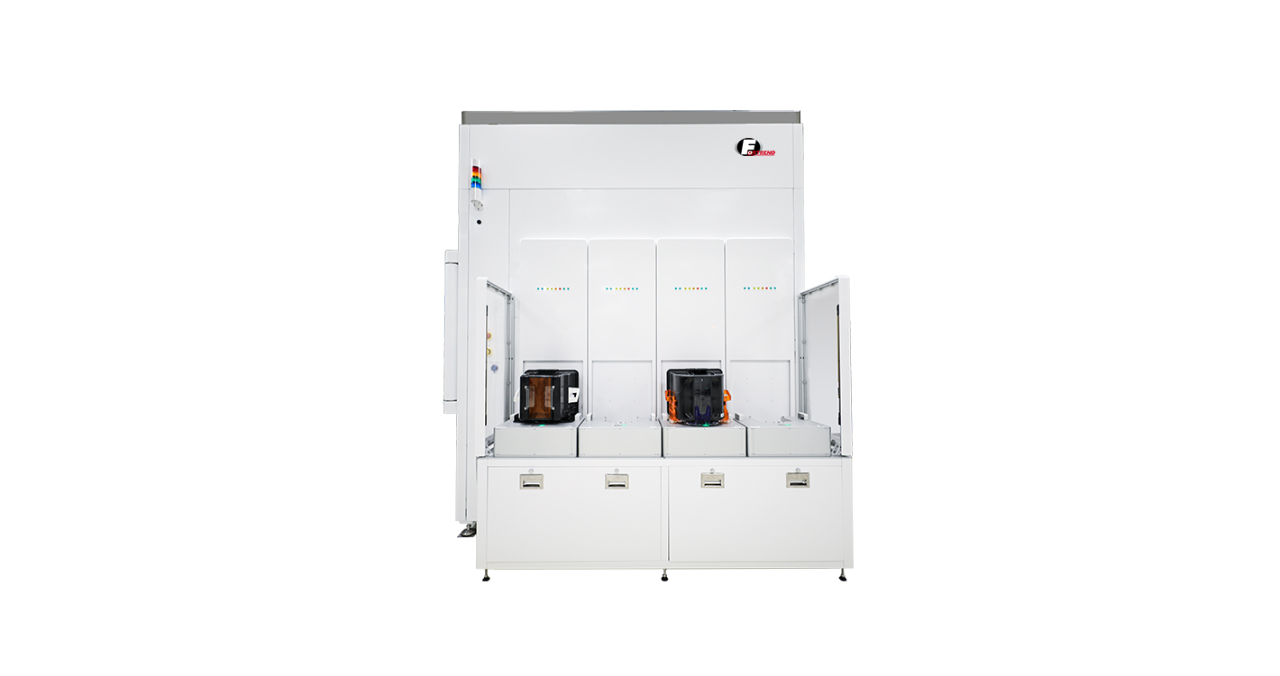
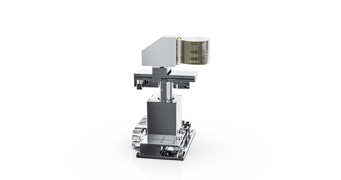
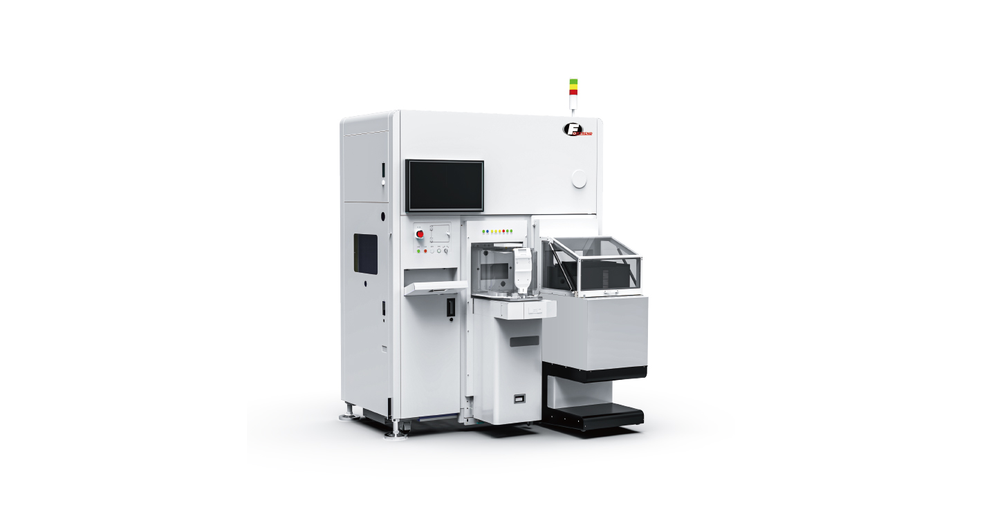
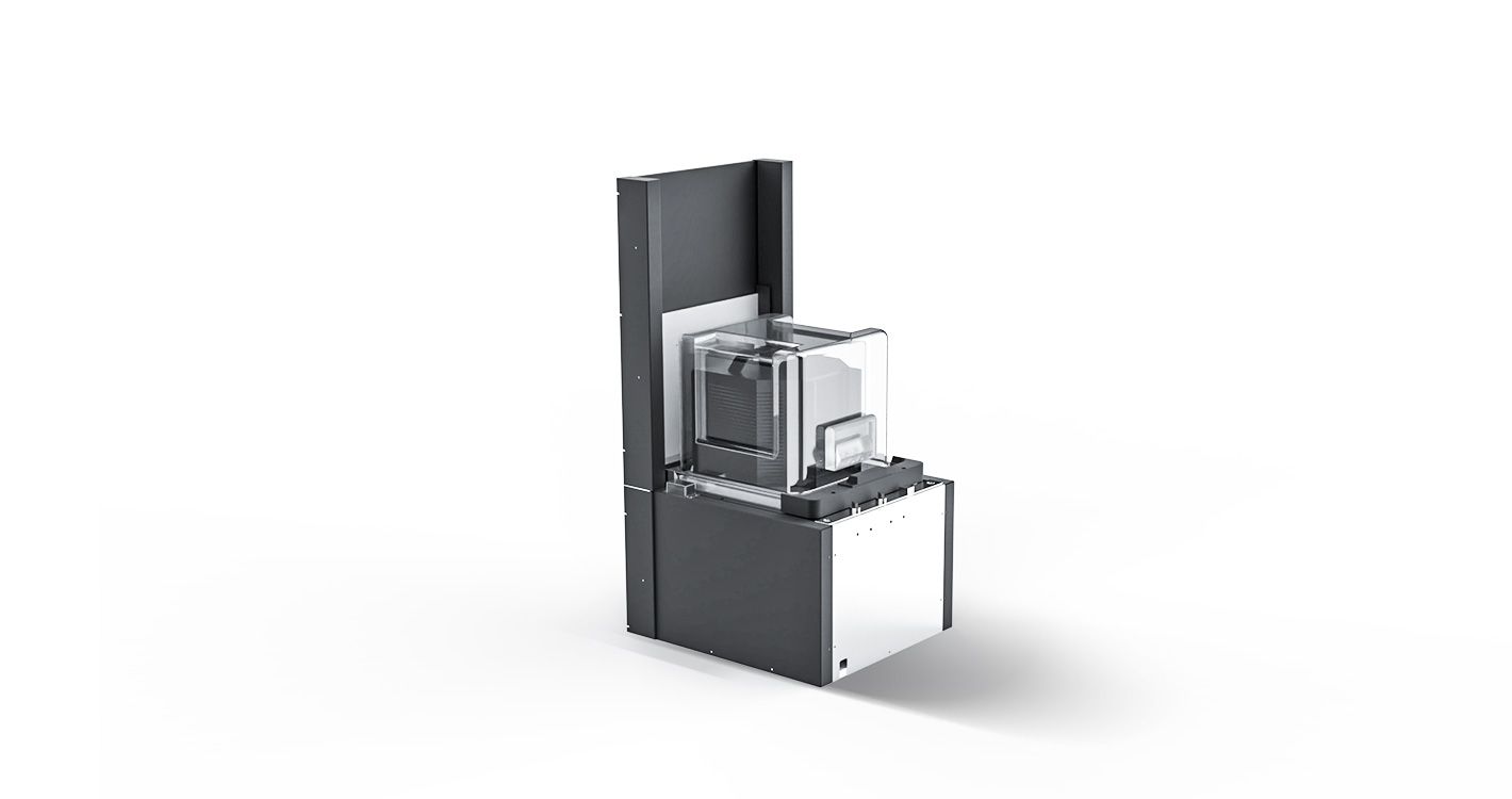
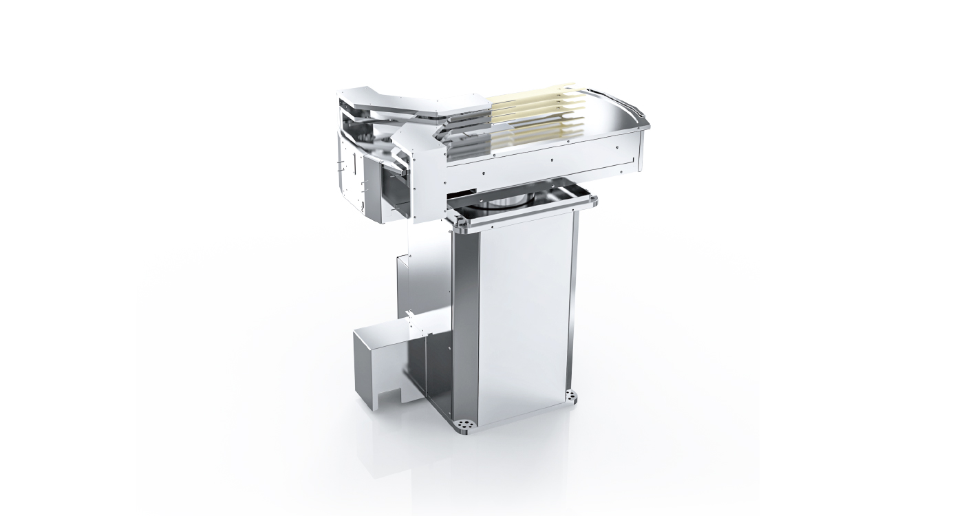
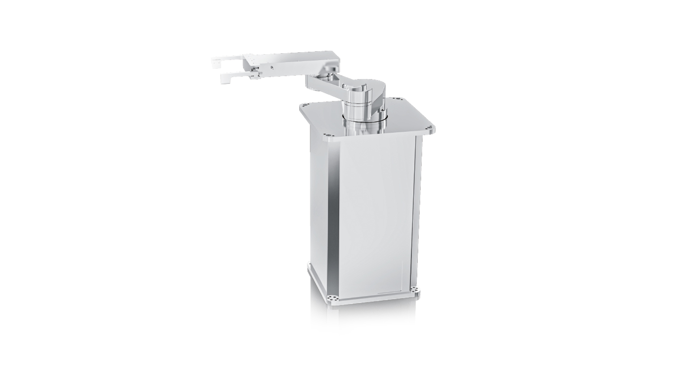
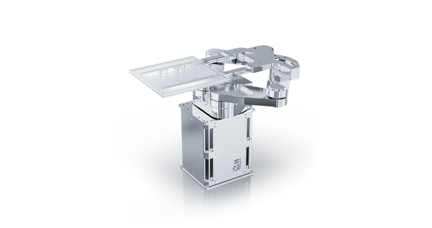
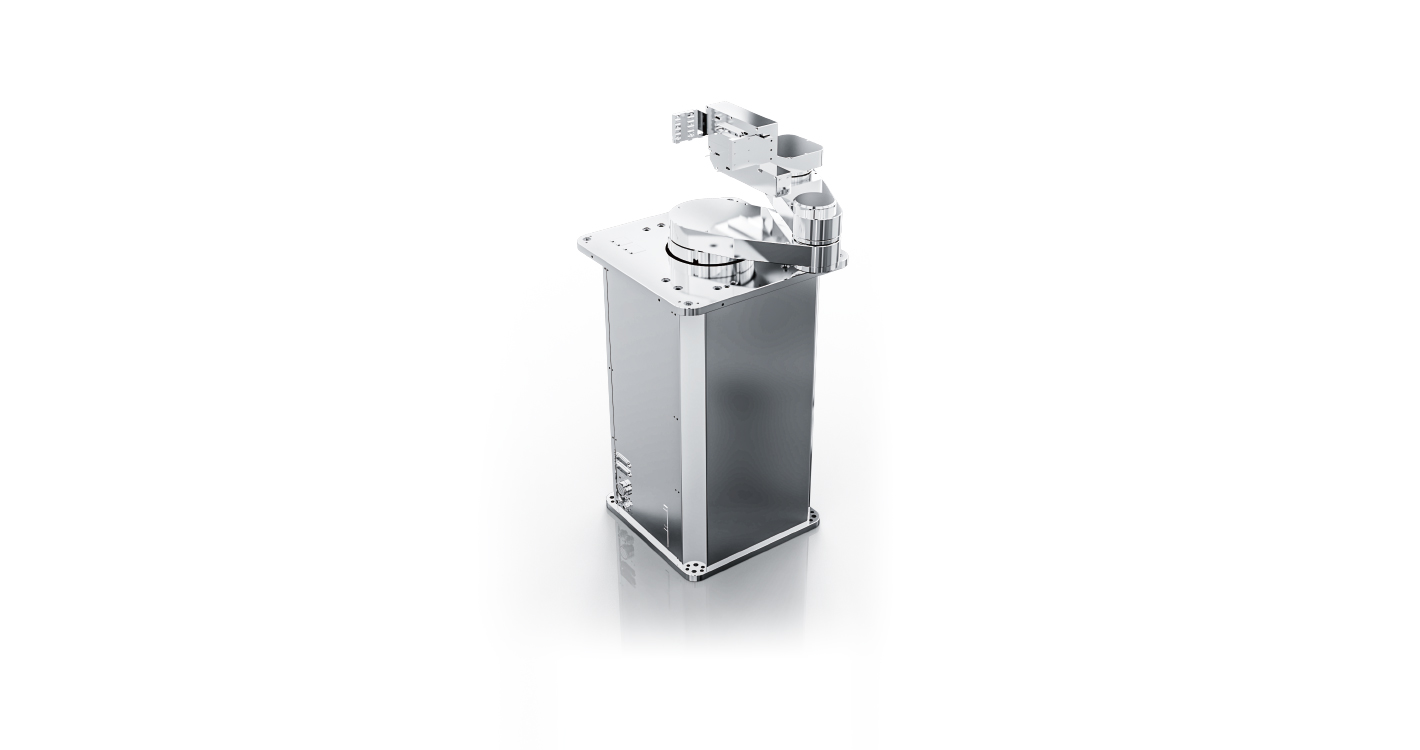
It supports both translucent and opaque wafer applications, suitable for silicon wafers and silicon carbide wafers with diameters ranging from 150 to 300mm.
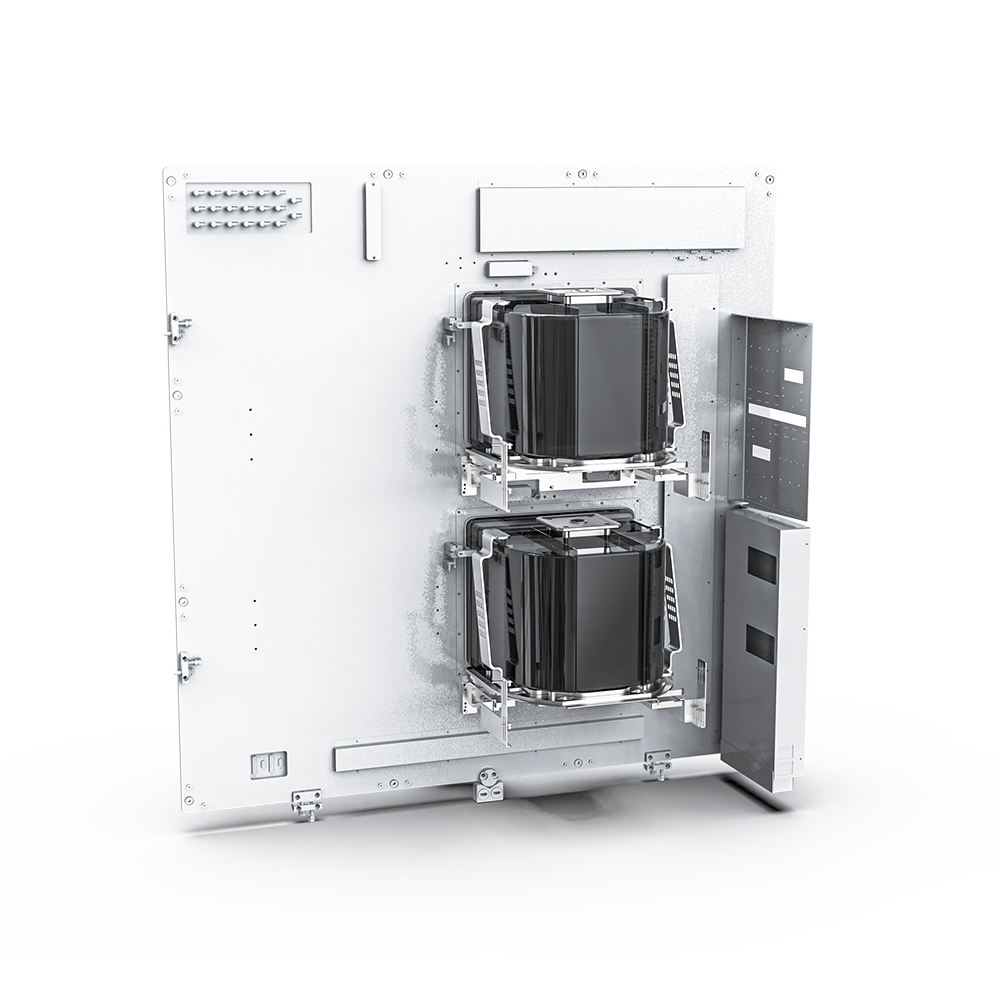
Integrated design with a built-in controller, eliminating the need for an additional controller and wiring space, achieving an ultra-compact size.
| Contents | Detail contents | Specification |
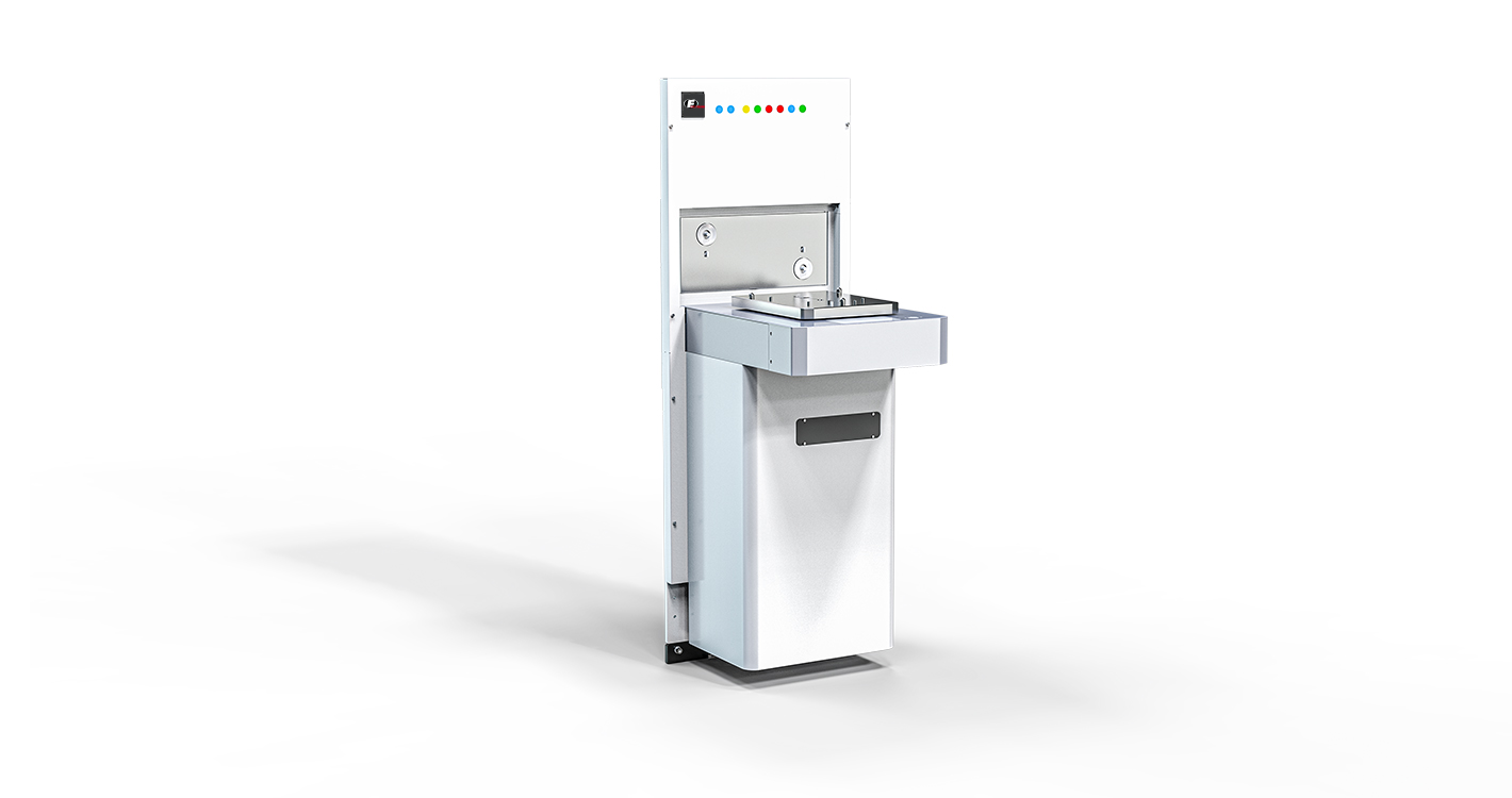
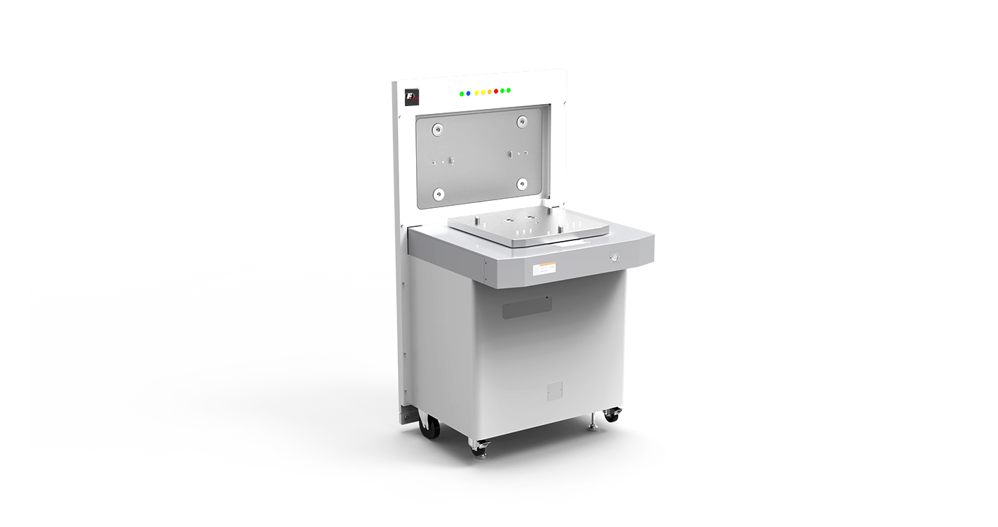
| Wafer Handing | Wafer handing size | 200/300 mm SEMI standard wafer |
| Alignment time | ≤3.2 sec(when handing 300mm wafer) | |
| Wafer off-center limit | Within ±5 mm | |
| Wafer holding method | Backside vacuum chuck | |
| Wafer holding check | Vacuum sensor with digital display | |
| Accuracy | Centering accuracy | ±0.1 mm |
| Rotation accuracy | ±0.1° | |
| Utility | Power | 24V DC±10%,5A |
| Vacuum | Less than -50kpa | |
| Communication | Serial R2-232C,parallel I/O | |
| Other | Weight | About 6 kgf |
| User interface | RS232C |
声明:本网站所展示产品外观、参数、性能描述、对比数据等均来自大族富创得内部实验室自有产品的检测和实验,仅供参考,以实物及实际参数为准,不做为法律依据。
021-34786180
service@fortrend.com.cn
上海市闵行区万芳路555号1号楼102、202室
.jpg)
二工位产品中心白底图1420x750.jpg)


二工位产品中心白底图1420x750.jpg)
.jpg)
2.jpg)